Today’s post is the translation of a speech Morris Chang delivered on the history and future of TSMC and the semiconductor industry at large in April. Chang is the founder and two-time CEO of TSMC, now 90-years-old and retired. The audience of the speech was Taiwanese government officials and business leaders. (See full video of original speech here.)
I wrote a tweet thread and full analysis of this speech in May, specifically on what Chang thought was the future competitive dynamic between TSMC/Taiwan, the US, China, and South Korea. (Spoiler alert: Chang believes Samsung of South Korea is the most fierce competitor of TSMC.)
Morris Chang, the now 90 years old founder of TSMC, gave a speech (in Mandarin) last week (ht @ruima)
— Kevin Xu (@kevinsxu) April 27, 2021
Among other things, he shared personal views on Taiwan's advantages + sized up competition from 🇺🇸🇨🇳🇰🇷
Thread of highlights + his slides in traditional Chinese👇 pic.twitter.com/SWaKHpARua
But there is so much more to this hour-long, exception-worthy speech, because Chang is the only person among the “founding fathers” of semiconductor technology still alive and lucid. Gordon Moore is alive, but as Chang noted in his speech, in poor health and retiring in Hawaii. Both Jack Kilby and Bob Noyce have passed away. All of these industry luminaries are Chang’s contemporaries, with whom Chang has gone to conferences in their younger days -- sharing dreams and ambitions over beers. Given how crucial understanding semiconductors is to the future of our world -- technologically and geopolitically -- it’s worth learning from one of the people who started it all, unfiltered.
In this translation are also screenshots of the slides (in traditional Chinese) Chang used during his speech. Just like what I did with our translation of Zhang Yiming’s last speech, I’ve bolded noteworthy phrases and passages throughout. I hope you enjoy reading and learning from it.

First of all, thank you very much, President Huang and Editor-in-Chief Fei of the Economic Daily News, for giving me this opportunity to speak on a topic that I have felt is very important in the past year or two. I would also like to thank all the distinguished guests who have come to speak here, Chairman Mark Liu and President CC Wei of TSMC, all the distinguished guests who have come to listen, and friends from the media.
Ladies and gentlemen, the title of my speech today is "Cherishing the Advantages of Taiwan's Semiconductor Wafer Manufacturing", and this speech is an appeal from me to the Taiwanese government, Taiwanese society, and TSMC.
My status is a TSMC retiree, and I no longer have any authority inside the company, which is my choosing, so TSMC is also a very important audience of what I’m advocating for in my speech today.
Because I already know that the vast majority of the audience is not in the tech community, much less the semiconductor community. So I would like to talk a little bit about the history of semiconductors, otherwise jumping straight into the key point —— the advantages of Taiwan's semiconductor wafer manufacturing —— might be too confusing.
This is the PowerPoint I made today. The first chapter starts with a brief history of semiconductors; the second chapter talks about the importance of semiconductors and why they have become a must-have for politicians and geopolitics. Then I will talk about the division of labor in the semiconductor industry. If it were not for this division of labor, we would not have the problems we have today. This division of labor started decades ago.
The fourth chapter will be the main topic - Taiwan's advantages in wafer manufacturing; the fifth one will be the fab-centered semiconductor industry chain, because the impact of wafer manufacturing on Taiwan is definitely not only on TSMC. TSMC’s wafer manufacturing has also driven a lot of other upstream, downstream and midstream industries.
Sixth, I’ll talk about the founding of the professional wafer manufacturing industry, that is, the founding of TSMC. This took people, opportunities, and a bit of luck or coincidence to happen (风云际会). It’s very rare so I think it’s hard to produce even one example from an entire generation. Seventh, TSMC's success; eighth, TSMC's status today; in the ninth, tenth, and eleventh chapters, I want to look at our foreign competitors, the United States, mainland China, and South Korea. These three are the most important competitors, although, of course, there are also Japan, Europe. However, because my topic today is wafer manufacturing, comparatively speaking, the United States, mainland China, and South Korea are our important competitors.
Finally, the twelfth point, since now people often say, "ah, we can have another so-called 'protective mountain of the nation'” (护国神山, i.e. an industry or company as influential to Taiwan as TSMC), I also want to talk about the possibility of producing the next "protective mountain of the nation." And lastly, the conclusion.
A Brief History of Semiconductors

The conductivity of a semiconductor is between that of a conductor (metal) and an insulator (wood). You can control the conductivity of the semiconductor. In short it is between metal and wood, so we call it semiconductor.
But honestly, until 1948, semiconductor was a term only known to scientists. Ordinary people, those who majored in liberal arts, business, or law didn’t know what it was. Only scientists, especially physicists, knew. So it was a very small group in society back then.
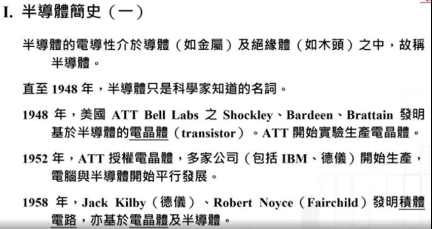
In 1948, a major event in the semiconductor industry took place. AT&T, at that time the largest telecommunications company in the United States, had Bell Labs under it, which was a world class research institution for many decades. There were three physicists at Bell Labs. Shockley was their leader, and Bardeen and Brattain didn't really like him, but the three of them collaborated to invent the transistors, which were based on semiconductors. What they invented was very important, and that was the transistor.
What is important is that it (semiconductor transistor) is very small. Prior to its invention, vacuum tubes could be used to make transistors, but vacuum tubes are big. During the Second World War when the United States began to manufacture computers, a computer was so large in size, because of the use of vacuum tubes, that it could occupy an entire room.
I came to the United States in 1949, and didn't see any computers the first year I was there. I was at Harvard, and the place where the computers were was far away from my freshman dormitory, so I didn't go. The next year, in 1950, I went to MIT, saw a computer, and learned to code. The computer was full of vacuum tubes, occupying the whole room. Honestly, the functionality of a computer as big as a room was not as powerful as the cell phone you are carrying today.
But anyway, the transistor was invented in 1948, and AT&T knew how important it was. These three physicists —— Shockley and Bardeen were theoretical physicists and Brattain was an applied physicist —— won the Nobel Physics Prize for transistors in 1956, pretty soon after the invention. Bardeen went on to win a second Nobel Prize, but that's not relevant to our topic today.
Shockley was born in the same year as my mother, and I was his student at Stanford University, where I listened to his lectures. He was a good lecturer, but the most memorable thing was his arrogance. Many students, including me, were afraid to ask him questions because when we saw other students asking him questions, the first thing he did was not to answer the question, but to taunt the student, looking down on him for asking a simple question and saying that his question was really ridiculous. In such a situation, few students dared to ask him questions and just listened to his lectures.
In 1952, AT&T knew that one company could not monopolize the transistor because it was too important for the future, so it licensed the technology to many companies, including IBM and Texas Instruments (TI). Many companies began to produce it, dozens of companies, including such large companies as GE. IBM was already quite big, but GE and RCA were even bigger than IBM. At that time, TI was a very small company, but it was also a licensee. It would become the most successful one in later decades to come.
After that, computers and semiconductors began to develop in parallel, because computers needed semiconductors the most.
I joined the semiconductor industry in 1955 after receiving my Master's degree from MIT. The history of semiconductors was irrelevant to me until 1955, and after 1955 the history of semiconductors merged with my life story.
In 1958, I had just arrived at TI. A new colleague of mine, who, like me, had just joined TI, was Jack Kilby. He was eight years older than me, but we were contemporaries. He was working on integrated circuits, which the chairman of TI asked him to do.
Jack Kilby was a very innovative person. His education level was not high —— only Master’s and no PhD. If you talked to him about theoretical physics, he wouldn’t understand it, but he was innovative. He insisted that he was an engineer, and whenever someone said he was a scientist, he would immediately deny it and say, "I am an engineer". He later invented the integrated circuit, which happened under my eyes.
That same year, Bob Noyce (or Robert Noyce) was at Fairchild, and I had just met Bob Noyce at that time. We were together at the Washington IEDM, a technical conference held in Washington every December. Noyce and Gordon Moore, who I will talk about later, were at Fairchild. I had already joined TI at that time, and I had just joined. We were quite gentlemanly at the conference together, and not aggressive with each other yet.
After the meeting, Noyce, Moore, and I went out for a beer in the evening, and at that time I was only 27, Noyce was only 31, and Moore was only 29. We were all young and excited, and thought we were the “Favored Children of Heaven” (天之骄子, i.e. children of destiny), lucky to have joined the promising field of semiconductors. After drinks and dinner, we sang our way back to the hotel from the restaurant amidst the snow drifts.
Both of them, Kilby and Noyce, invented the integrated circuit almost at the same time. In fact, Kilby was a little earlier, about a month or two earlier. But honestly, although Kilby's was a little earlier, Noyce's was a planar construction while Kilby's was a bonded construction. Without Noyce's planar construction, integrated circuits would not have been made.
Later, after some legal disputes in the court or something, both sides —— TI and Fairchild —— settled, saying that the two people jointly invented the integrated circuit. Noyce unfortunately passed away very early, in 1990, at the age of 63. He lived a full life: had a lot of girlfriends, often flew his own plane, went diving and swimming, and played many other sports.

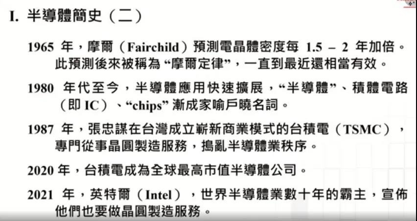
I think the next important thing (in semiconductor history) was Moore’s Law in 1965. Moore, at Fairchild, predicted that circuit density would double every 1.5 - 2 years, a prediction that came to be known as "Moore's Law" and remained quite valid until recently.
It’s been decades. Although Moore's Law is only a prediction, it has forced every company to double the circuit density every year and a half to two years, because by then the semiconductor industry was no longer gentlemanly —— companies already became aggressively competitive —— and everyone thought, “If I don’t double it, my competitors will.” So they tried their very best to do so. This was the important thing about Moore's Law. It was at first only a prediction, which might not have been true. In fact, if MOS (metal–oxide–semiconductor) was not invented, or I should say made practical, since it had existed, Moore's Law would not have been accurate. That was after Moore's Law was published, in around 1968, 1969.
Almost ten years ago, IEDM —— the same conference that I went to 50 years ago and sang my way back to the hotel —— invited me to speak on the biggest semiconductor innovations. I then put transistors and integrated circuits in the speech. I also put Moore's Law in it, because of what I just said, the pressure (to double the circuit density every 1.5 - 2 years). I also put MOS in it. MOS allows us to (let the circuit density) double, double, and double again. Lastly, I included chip foundry in the speech —— it was also listed as one of the important innovations in the history of the semiconductor industry.
From the 1980s to the present, semiconductor applications expanded rapidly, mainly PCs, and later, of course, cell phones etc. Why do I talk about the year of 1980? Because 1980 was when IBM released its PC, which universalized PCs. IBM was a big company at that time, so when people saw that IBM released a PC, they saw the PC as a legitimate thing, not just a toy. Before IBM, Apple and several small companies already came out with PCs, but people said, “hey, this might just be a toy.” IBM’s PC release in 1980 changed this notion.
Especially in the 90s. In the 80s, IBM came out and PCs became prevalent in the office, but in the 90s they became prevalent at home. Even housewives used them. I personally experienced this history and so had a deep impression of it. The 90s was also Andy Grove's era. Everyone always thinks that he is Intel's best, greatest CEO ever. This is really a case of, “Our times shape our heroes. Our heroes shape our times” (时势造英雄,英雄造时势). The 90s was the era of very rapid PC adoption, and Intel was almost exclusive in making processors, so the situation made Andy Grove a hero.
In 1987, Morris Chang established TSMC in Taiwan with a new business model, specializing in wafer manufacturing services. This was a disruptive innovation that disrupted the semiconductor industry, and I'll explain why in a moment. In 2020, TSMC became the world's largest semiconductor company by market capitalization.
Intel was the dominant player in the world's semiconductor industry for decades, from the late 1980s until recently. TI's period of dominance was from the 60s to mid-80s. Last year, TSMC reached its highest market cap at $600 billion, when Intel had just over $200 billion, less than half of TSMC. However, what will happen after this is not certain.
In 2021, Intel, the former dominant player, announced that they are also going to provide wafer manufacturing services. This is quite ironic to me. Originally they were the dominant player, and frankly they looked down on wafer manufacturing, thinking that this thing couldn't do much. I was acquainted with them, so at first I sought investment from Intel. At that time, in 1985, TSMC was raising capital, but the timing was not right and the economy was not good, so Intel refused to invest.
However, after TSMC was established, Intel, Andy Grove, and Gordon Moore helped a lot, but they never thought that this foundry business model would become so important; nor did they ever think that one day they would also do wafer manufacturing. Of course, Gordon Moore is now in very bad health and lives on Big Island, Hawaii. Noyce, as I just said, has died, and Andy Grove has also passed away.
Importance of Semiconductors
I’ve talked about history for a long time, so now we can go a little faster. The importance of semiconductors can be first of all seen in national defense: missile navigation, GPS, this is another small story.
Now we are very familiar with GPS because all the cars have it. The first time I heard about GPS was at TI. I had top-secret clearance at TI, and was in charge of semiconductors. TI had a defence system division and they needed integrated circuits to do GPS to navigate the missile. I heard them talk about it and thought that it was super cool, “how can it hit within 5 ft diameter of a target from thousands of miles away?” This was in the 70s. Now every car has GPS.
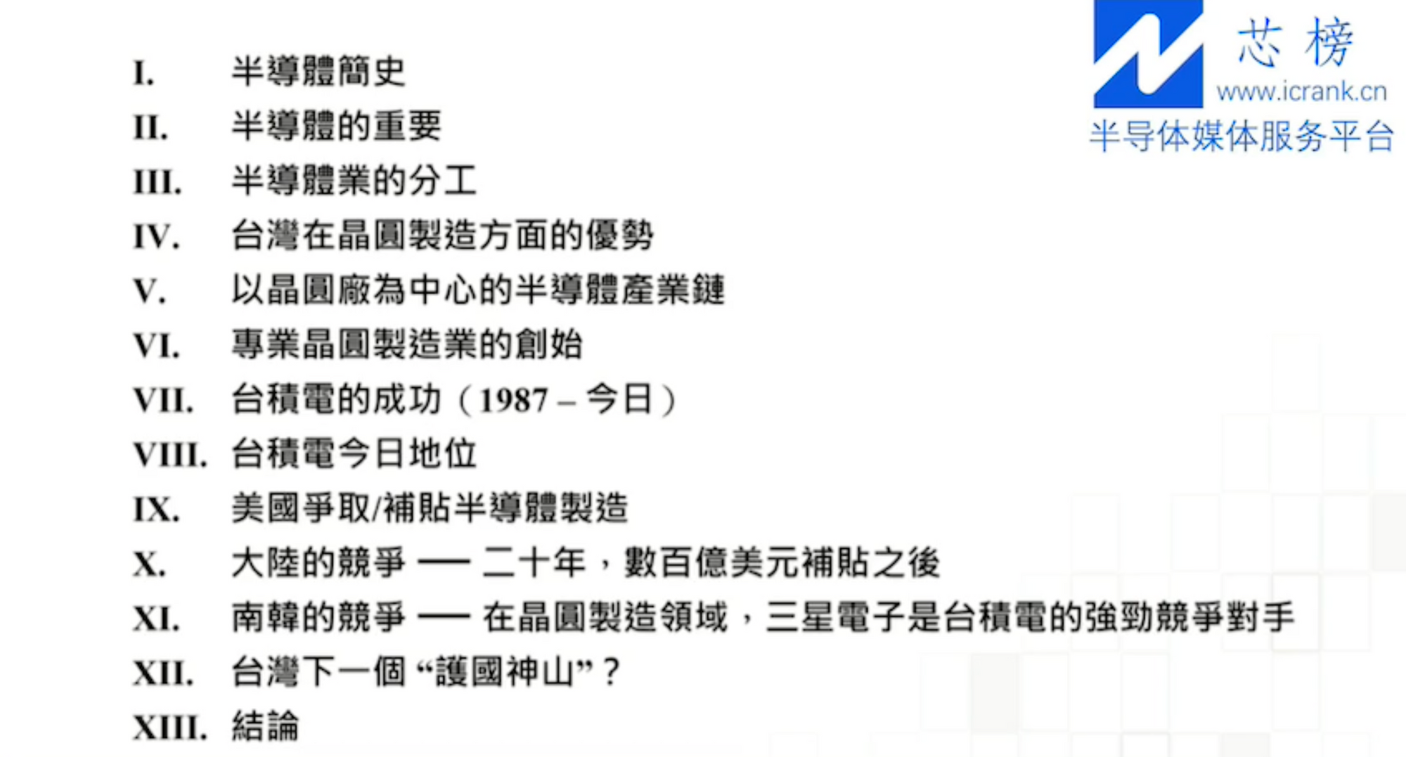
Semiconductors are ubiquitous now, in commerce, industry, and daily life, from computers to cell phones. And of course, Covid19 has accelerated the global digital transformation.
Division of Labor in the Semiconductor Industry
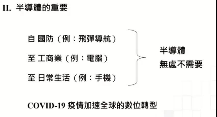
Originally, when I first joined the semiconductor field in 1955, there was no division of labor in the industry. Every company did everything by themselves. They did IC design —— sorry, there was no IC in 1955. It was transistors, but a few years later there would be IC. IC design needed design tools, but each company would do it on their own. Design is actually quite technology-intensive, the added value is also quite high, but it’s not so capital-intensive, so it doesn’t require a lot of capital. Process R&D and wafer manufacturing are capital-intensive, technology-intensive, and have high added value. The technology and capital required for packaging & testing are not as intensive as that for wafer manufacturing. Compared to IC design, packaging & testing is more capital-intensive but not as technology-intensive. In short, every semiconductor company did its own thing.
The division of labor can be said to have begun in the 1960s and the first to have been separated out was packaging & testing. Companies often still did it themselves, but in low-wage areas, such as Taiwan, the Philippines, Singapore, Hong Kong (Hong Kong was where they started), and even Japan. In the 60s, you know that Japan's wages were only 5% of that in the United States. At that time, I suggested that TI come to Taiwan, and the CEO of TI said, "Let's go to Japan, because the salary in Japan is only 5%. In Taiwan it’s only 1%, but the difference between 1% and 5% is not big.” However, I told him at that time that Japan's wages would rise quickly, while Taiwan's wages would not rise so fast, so he came to Taiwan. This is just a small anecdote.
In short, packaging & testing in the 60s was at first not technically separated out, but done by individual companies in low-wage regions. However, in low-wage areas, you couldn’t lock up the market and have it all to yourself. Low-wage areas also had entrepreneurs. And regardless of whether you were TI or Motorola, they saw that you engaged in packaging & testing here. They knew that this technology was not that difficult, so they would open companies that had lower overhead than you and would say, "hey, you should let us do it for you". That’s why there are a lot of packaging facilities in Korea and so on.
It was like that in the semiconductor industry till 1985. I was in New York at General Instrument then. Gordon Campbell was a pretty famous entrepreneur who had founded a semiconductor company that was quite successful. In 1984, he had just sold it and wanted to build a new company. I didn't really know Gordon Campbell, but I knew his name, and he knew my name. He said, "I'm hoping that you and General Instrument can invest [in my new company]. Can you come and take a look?”
So we made an appointment, and he came to see me and said he needed $50 million. I said, "Do you have a business plan?" He said, "The business plan is all in my head.” Then I said, "Even if I want to invest in your company, I have to report this to General Instrument's board of directors. There must be a business plan.” He said, “No problem, no problem Morris. I'll send it to you in two weeks.”
He went back —— he was in California while I was in New York —— but 3 weeks passed and nothing happened. I was actually quite interested, so I called him. He said, "I'm sorry Morris, I didn't contact you again because I don't need 50 million anymore. I just need 5 million, 5 million is enough, and I can get that together myself. ” When I asked why, he said, “I’m not going to do wafer manufacturing —— that is capital intensive —— I will just build a design company.”
This was the first time I had heard of a company specializing only in design. Of course, the complementary part of that is wafer manufacturing: since there are companies specializing in design, there can also be companies specializing in wafer manufacturing. It took me a year to figure out this complementary model, which became TSMC. Anyway, I originally thought this speech would be too short, but it seems too long now.
Why is this business model so disruptive? Because process R&D and wafer manufacturing are in fact the heart of the so-called IDM (integrated device manufacturer). Packaging & testing can be separated out, but process R&D and wafer manufacturing are at least part of the heart, the other part being IC design.
TSMC's business model is that semiconductor companies are our customers, our friends. This is the biggest discovery of this business model. The biggest discovery of a business model is who your customer is and how you make money. Since our customers are semiconductor companies, if they originally make their own wafer but now we make wafer too, then our competitors are those in charge of wafer manufacturing inside semiconductor companies. That's why it's very disruptive. You young listeners haven't experienced this kind of corporate politics —— this is very disruptive.
Taiwan’s Advantages in Wafer Manufacturing

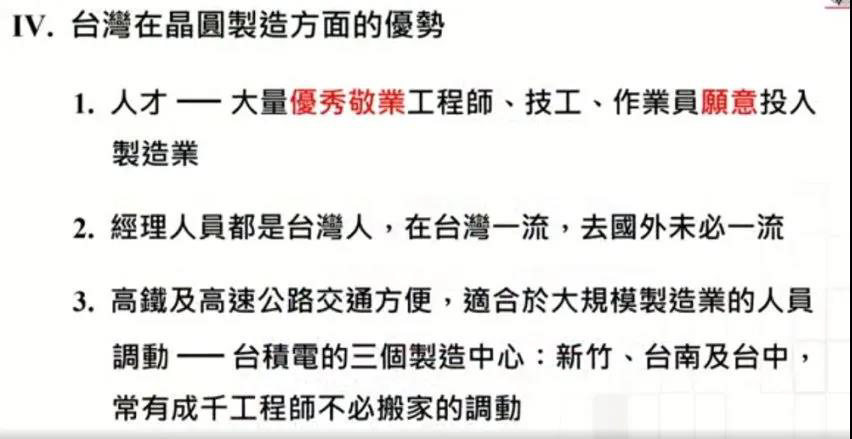
First of all, we have talent, a large number of excellent and dedicated engineers, technicians, operators willing to commit to manufacturing. This is very important. At least in the United States, engineers are not as dedicated as those in Taiwan. I think people in other professions as well, haha. Americans are not as dedicated as Taiwanese.
So what I want now are excellent and dedicated engineers, technicians, and operators, all of whom are important and need to be willing to commit to the manufacturing industry. Manufacturing in America is no longer a “hot” industry. It has not been “hot” for decades. People don’t want to work in the manufacturing industry. There are a lot of nerds doing R&D; there are a lot of people in the financial sector —— engineers etc. can also be in the financial sector and do venture capital and private equity. There are also many people doing marketing. All of the above (i.e. R&D, finance, marketing) are more desirable fields to be in than manufacturing. The commitment to manufacturing is a great advantage of Taiwan.
Secondly, our managers are Taiwanese. In Taiwan they’re the best, but they may not be the best when working overseas. So is the reverse —— my own experience demonstrates this. I worked for two or three decades in the United States to reach the level just below the CEO of a large company, but coming back here to Taiwan, even managing teams of a much smaller scale messes up my brain. Culture, habits, and language are all different. Although I had been speaking Chinese till I was 18, 36 years of not using it made it a problem for me to speak it again at the age of 54. I’m afraid it’s probably still a problem today, haha.
Another advantage Taiwan has is its convenient high-speed rail and highway transportation system, which makes mass manufacturing personnel movement easy. TSMC's three manufacturing centers —— Hsinchu, Tainan, and Taichung —— often have thousands of engineers whose location assignment changes but who do not have to move their family. They can be transferred from Tainan to Taichung, or Hsinchu to Taichung. The time from Tainan to Hsinchu is a little longer, so that’s not a one-day commute anymore, but the commute between Taichung and Tainan, and Hsinchu and Taichung, are within a day. Even when transportation is convenient, TSMC also has dormitories so that engineers can have a place to stay during the week and go home on weekends. They don’t have to move their whole family when their new assignment is often only a year. How do you do that in Arizona?
Fab-Centered Semiconductor Industry Chain
Okay next slide. TSMC is definitely not the only company in the industry. There are design companies like MediaTek —— perhaps the largest among all but there are many more. Midstream in the industry chain are Taiwanese equipment manufacturers: silicon wafers, gas suppliers, raw materials and so on. There are also important global semiconductor equipment vendors, such as ASML, Applied Materials, LAM Research, etc. all of which have service bases, training centers, and R&D laboratories in Taiwan. They are brought here by TSMC. Of course, I’m talking about TSMC today, but there are other wafer manufacturing companies in Taiwan besides it. Downstream are assembly and testing companies, so there is a fairly complete industry supply chain in Taiwan.
Origin of Professional Wafer Manufacturing

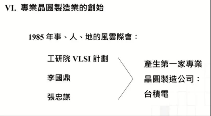
How did the professional wafer manufacturing model come about? It was a coincidence of events, places, and people in 1985 (风云际会). The “event” was the VLSI program of ITRI (Taiwan’s Industrial Technology Research Institute), which had been in operation for ten years at that point, and frankly speaking, it was at the end of its rope. It needed a lot of funding every year, but whenever it tried to do some small business, people would say that it was competing against the people of Taiwan for profit.
At the beginning, its technology was only one generation behind the world's most advanced technology. ITRI took RCA’s technology in 1975, but RCA itself was not first-class at that time, so the technology ITRI brought back was already behind. After ten years of working on it, the gap became even bigger. They were then two or three generations behind. It also cost quite a lot to employ hundreds of people. If it did some small business, it was accused of competing against the Taiwanese people for profit.
So Mr. Li Kwoh-ting wanted to find a way out, and I took advantage of that opportunity. This was definitely not hitchhiking. The foundry model was the world's first. Although the upside was that there were no competitors, the downside was that there were no customers either. I’m not going to talk about this today.
TSMC’s Success
Why did TSMC succeed? What are the factors behind it? The most important factors are what I’ve just talked about: Taiwan’s advantages in wafer manufacturing.
Of course professional managerial leadership is important too. I think TSMC is the largest company in Taiwan and led by professional managers, everyone from the chairman down. Of course, there are disadvantages as well, but I do think that to set up a world-class enterprise, deploying a professional managerial leadership is still a better model.
We have been investing in R&D for a long time as well. This is what we’ve done and important for our success.
We’ve also had 120,000 employees since our founding, including those who have left. This actually indicates a very low turnover rate, only about 3%, 4%. We currently have 50,000 employees and have only had 120,000 employees in total for the past 30 years.
Of course, the support from the government and society at large is very important to TSMC’s success as well. This is what I’m calling for today. I hope they will continue to support TSMC and increase the advantages of Taiwan.
Status of TSMC Today
TSMC’s status today is the leader in semiconductor manufacturing technology.
The semiconductor market was $476 billion last year, of which memory chip was $117 billion and logic chip was $359 billion. About a quarter of that, actually just a quarter, was made by TSMC.
Almost everyone in the developed world, about 2.5 billion people, uses semiconductor products made by TSMC in their daily life or work.
For example, I actually wear a hearing aid, and I recently discovered that the integrated circuits inside the hearing aid are also made by TSMC.
Every 3 years, the hearing aid salesman comes over and tells me about the new model and asks me to buy another set. I always asked him what the benefits of the new model were, and he said a bunch of things, and then he told me that the ICs were replaced so they would function better. I actually listened to him and bought 3 or 4 of them.
Although the integrated circuit has improved over the generations, it doesn't seem to help the function of the hearing aids much, to be honest. It's kind of like the American cars, with new models every year.
The US Subsidizing Semiconductor Manufacturing
Now let’s look at the countries we are competing against. The United States is the most powerful, with its subsidies.
Comparing the American wafer manufacturing conditions with Taiwan, land is America’s absolute advantage. So are water and electricity. However, Taiwan’s advantages that I just talked about are America’s weaknesses.
American talents are not as good as Taiwanese ones, whether it’s engineers, technicians, foremen, or operators. The personnel dispatched by Taiwan to the US, like I said, are not necessarily the best in terms of management ability. The US also lacks the ability to mobilize manufacturing personnel on a large scale.
The result is that the unit cost is significantly higher in the US than in Taiwan. It’s true that it has subsidies. The US has both the carrot and the stick, with the former being federal and state government financial subsidies. However, short-term subsidies can not make up for its long-term competitive disadvantages.
The subsidies only last for a few years, but you still have to keep going after those years.
Competition from Mainland China: After 20 Years and Tens of Billions in Subsidies

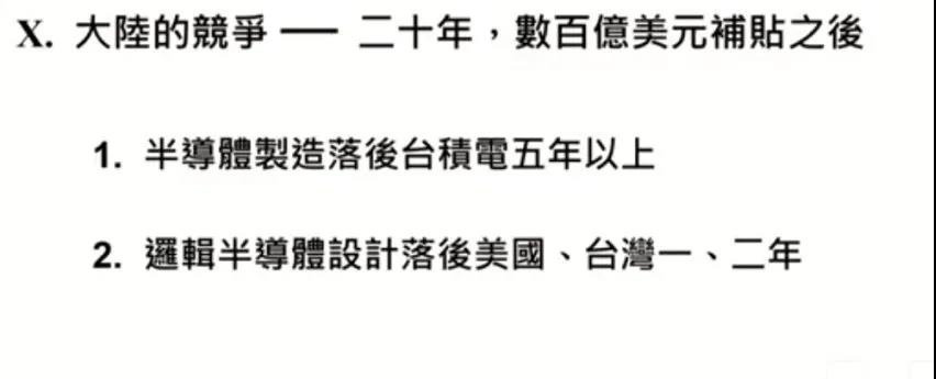
Next, competition from mainland China. After 20 years and tens of billions of dollars in subsidies, semiconductor manufacturing in China is more than 5 years behind TSMC. Logic semiconductor design is 1-2 years behind the United States and Taiwan.
Mainland is not yet a rival, especially in terms of wafer manufacturing.
Competition from South Korea: In Wafer Manufacturing, Samsung Electronics is a Strong Competitor

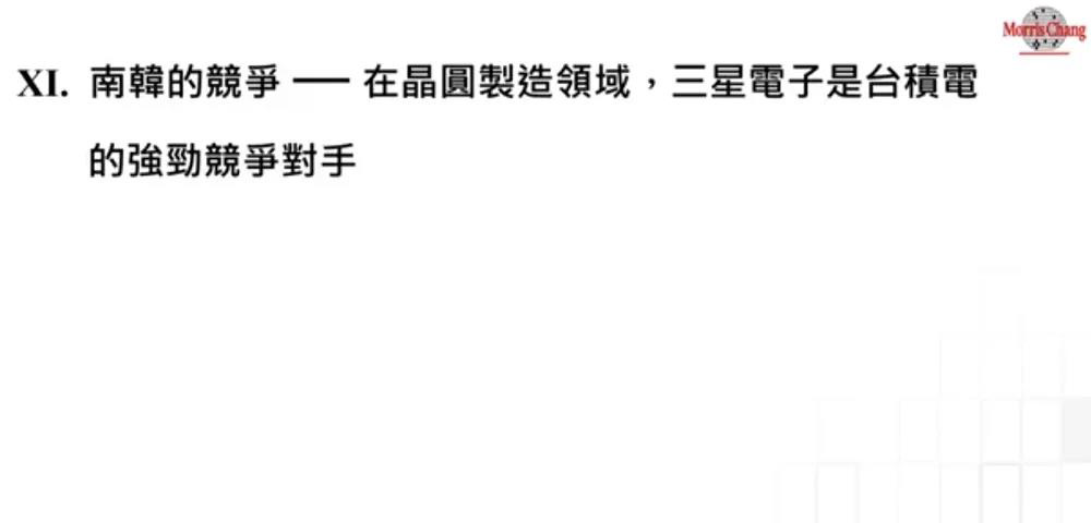
As for South Korea's competition in the field of wafer manufacturing, Samsung Electronics is a strong competitor of TSMC.
Why? Because the advantages of South Korea in wafer manufacturing and Taiwan are similar, from talent to the ease of transporting personnel, since Samsung’s factories are all in one place.
Its managers are also Korean, first-class in South Korea but not necessarily abroad.
Taiwan’s Next “Protective Mountain of the Nation”

Some people are now saying that we have a "protective mountain of the nation". If the definition of that is an industry that is important to the world and Taiwan has a high market share, then you need to find an industry where Taiwan has potential advantages and it’s important to the world.
Otherwise, Taiwan only has 24 million people and is a small place. I found wafer fabrication as a protective mountain of the nation, but I have not found a second one, and I have been searching for decades.
Then the next "protective mountain of the nation" needs to have an innovative product or business model, like wafer manufacturing/foundry, which was a new business model.
Then you also need many years of effort and business operations.To answer this question, my answer is: difficult!
Conclusion
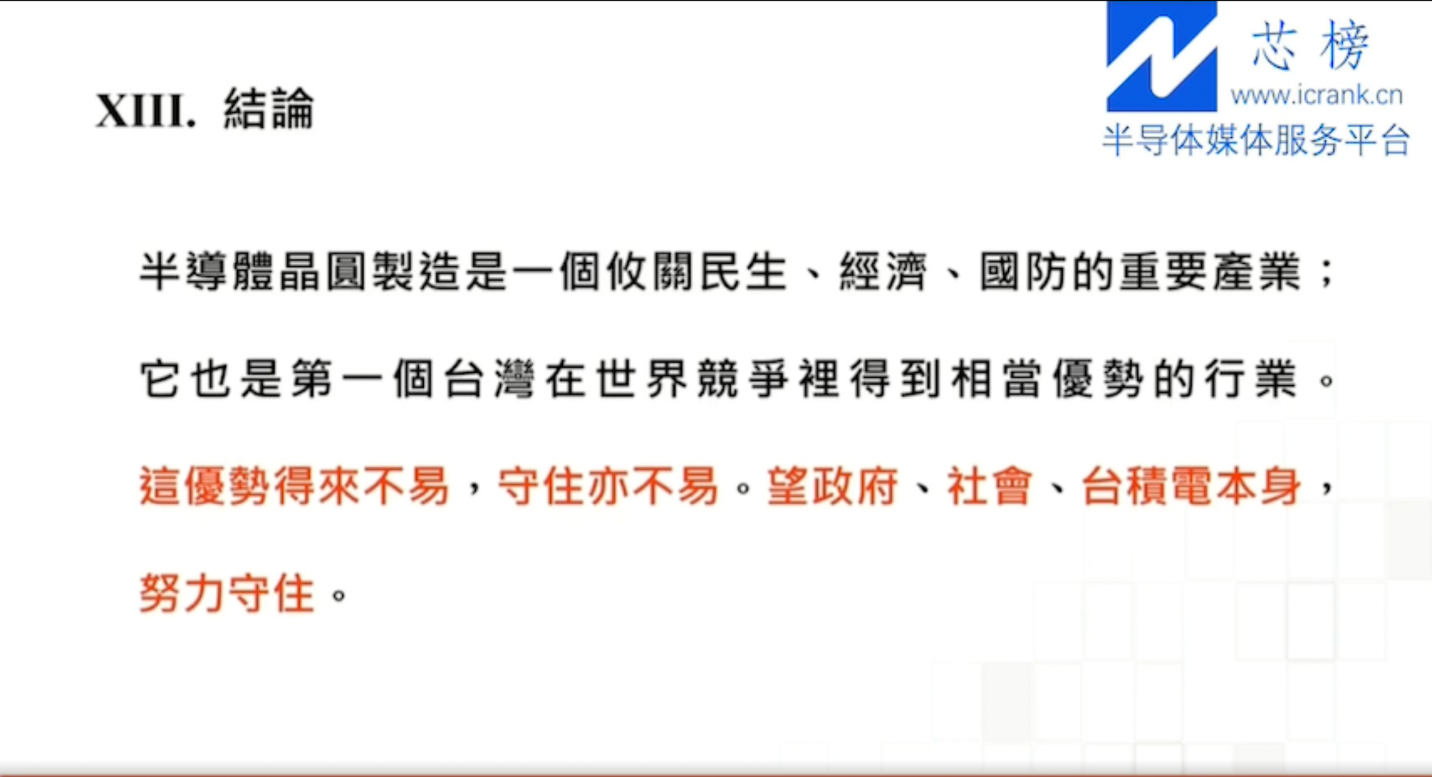
Semiconductor wafer manufacturing is an important industry that impacts people's livelihood, economy, and national defense. It is also the first industry in which Taiwan has gained considerable advantages in world competitiveness. These advantages are not easy to obtain or keep. I hope that the government, society, and TSMC itself will make efforts to protect them.
This is my appeal to you today. Thank you.
To read all previous posts, please check out the Archive section. New content will be delivered to your inbox once a week. Follow and interact with me on: Twitter, LinkedIn, Clubhouse (@kevinsxu).
张忠谋的最后一次演讲
今天的文章是张忠谋在4月份发表的关于台积电和整个半导体行业的历史和未来的演讲全文。张忠谋即是台积电的创始人和两任CEO,现在90岁了,已经退休。演讲的听众是台湾政府官员和商界领袖。(请点击这里看演讲的完整视频)。
5月份的时候,我写了几条推特和对演讲的全面分析文章,尤其关于张忠谋对台积电/台湾、美国、中国和韩国之间在半导体领域未来竞争走向的看法。(剧透:张忠谋认为韩国的三星是台积电最有竞争力的对手。)
Morris Chang, the now 90 years old founder of TSMC, gave a speech (in Mandarin) last week (ht @ruima)
— Kevin Xu (@kevinsxu) April 27, 2021
Among other things, he shared personal views on Taiwan's advantages + sized up competition from 🇺🇸🇨🇳🇰🇷
Thread of highlights + his slides in traditional Chinese👇 pic.twitter.com/SWaKHpARua
但此演讲中,还有很多极有价值的内容。张忠谋是半导体技术 "奠基人" 中唯一仍然活着且头脑清醒的人。Gordon Moore虽然还活着,但正如张忠谋在演讲中提到的,健康状况已不佳,在夏威夷退休。Jack Kilby和Bob Noyce都已去世。所有这些业界元老都张忠谋的同龄人,在年轻时与他们一起参加会议,喝啤酒,分享各自的梦想和雄心。鉴于了解半导体对我们世界的未来 -- 无论是科技上,还是地缘政治关系上 -- 都极为重要,需要从张忠谋的言辞中毫无过滤的 了解这个行业的历史和未来。
在这篇演讲全文中,间插了张忠谋当时演讲时用的ppt的截图(繁体)。希望阅读这篇演讲对您有帮助,有启发。
经济日报的黄社长,费总编辑,非常谢谢你们给我这个机会来讲一个我这一两年感觉非常重要的话题。各位到这来演讲的贵宾,台积电的Mark刘董事长以及CC Wei魏总裁,所有来听的贵宾们,还有媒体的朋友们,各位女士,各位先生。
今天我的题目是《珍惜台湾半导体晶圆制造的优势》,这个演讲是我的一个呼吁,对台湾政府、台湾社会、以及台积电的呼吁。
我的身份是一个退休的台积电(人员),在公司里面已经没有权力,这也是我选择的,所以说,这个呼吁,台积电也是一个非常重要的对象。
因为我已经知道,听众绝大部分都不是在资讯界,更不是在半导体界。所以,我想把半导体的历史稍微讲一下,不然马上跳进重要的点 —— 台湾半导体晶圆制造的优势 —— 我想大家不会很了解。

这个是我今天做的 PowerPoint,第一章先讲半导体简史;第二章讲半导体的重要性,为什么半导体已经变成地缘政治家的必争之地。那我又讲讲半导体业的分工,假如不是为了这个分工,我们今天不会有这个问题,这个分工是几十年以前就开始了。
第四个就进入正题了 —— 台湾在晶圆制造方面的优势;第五讲晶圆厂为中心的半导体产业园,因为晶圆制造对台湾的影响绝对不只是台积电一家。台积电,晶圆制造也带动了很多的别的上游、下游以及中游的产业。
第六,讲一下专业晶圆制造业的创始,也就是台积电的创始。这个其实是风云际会,很难得的风云际会,我想一代里头出不了一个;第七,台积电的成功;第八台积电今日的地位;第九、第十跟第十一我要看看我们国外的竞争者,美国、大陆、南韩,这三个是最重要的竞争者,当然也有日本、欧洲,但是因为我说的是晶圆制造,比较起来美国、大陆跟南韩是我们重要的竞争者。
最后,第十二点,因为现在社会上也常说,“啊,我们可以再来一个所谓‘护国神山’”,那我也要谈谈下一个“护国神山”的可能。最下面(最后是)结论。
半导体简史
半导体的电导性介于导体(也就是金属)与绝缘体(也就是木头)。你可以控制半导体的电导性,总之它是介于金属和木头之间,所以称为半导体。
不过老实说,一直到 1948 年,半导体(semiconductor)只是一个科学家知道的名词。老百姓不知道的,念文科的、念商科的、念法律的也不知道。科学家,尤其是物理学家,他们知道,是社会上很少一群。
1948 年,一件半导体业的大事发生了。美国的 AT&T 公司,那个时候是美国最大的电信公司。它下面有贝尔实验室,好几十年都是世界第一流的研究机构。贝尔实验室里有三位物理学家,Shockley 是他们的领袖,Bardeen 和 Brattain 两位不太服他,可是他们三个还是合作发明了基于半导体的电晶体。他们发明的东西是非常重要的,就是 transistor.
那重要的是什么呢?是它(半导体电晶体的体积)非常小。以前是真空管可以做 transistor,但是真空管大得很,在第二次世界大战的时候美国就要制造计算机,那个计算机是大的要命的,因为使用了真空管,(计算机要占)整个房间。
我1949年到美国,我到美国第一年没有看到任何计算机。我在哈佛,要看到计算机的地方离我大一的宿舍远得很呢,没有去看。第二年1950 年,我到麻省理工了,就看到计算机了,而且还学编程了什么的。那个计算机都是真空管,整个房间。老实说,整个房间那么大的计算机的功能还不如你们身上带的手机喔。
不过总之,1948年 transistor 发明了,AT&T 知道它的重要性,这三个物理学家 —— Shockley和Bardeen是理论物理学家,Brattain是实验物理学家 —— 这三个人后来 1956 年,蛮快的,就因为这个发明获得了诺贝尔物理学奖。Bardeen后来还得了第二个诺贝尔奖,可是那个跟我们今天的题目无关了。
Shockley与我妈妈同年,我是他的学生,在斯坦福大学,听他讲课。讲课讲得不错,但最令人难忘的是他的傲慢。许多学生,包括我,不敢问他问题,因为我们看到别的学生问他问题时,他首先不是回答这个问题,而是奚落这个学生一番,看不起他问很多简单的问题,表示你的问题实在是可笑。这样的情形下,所以很少有学生敢问他问题,只是听他的课。
1952 年,AT&T 知道不能一个公司独占 transistor,因为这个东西以后太重要了,它就自动把这个授权出来给许多公司,包括 IBM、德仪(德州仪器,TI),那许多公司就开始生产了,几十家公司,也包括GE这种大的公司。IBM当然已经相当大了,可是GE, RCA那个时候比IBM更大。当时德仪是非常小的公司,可是它也是一个licensee. 那后来几十年的光景,它最成功。
之后,电脑和半导体就开始平行发展,因为电脑是最需要半导体的。
我是在1955年得到麻省理工Master学位(硕士研究生学位)以后,就加入了半导体行业。半导体的历史一直到1955年可以说是跟我无关,1955年以后半导体的历史就和我自传就merge起来了。
1958年,那一年我刚刚到德仪。我的一个新同事,他也和我一样,刚刚加入德仪,他叫杰克・基尔比(Jack Kilby),他比我大八岁,但是我们是同代人(contemporaries)。他在做积体电路(integrated circuit,也叫集成电路),是德仪董事长叫他做的。
Jack Kilby是个非常innovative的人,他的学历不高,只有Master,没有 PhD(学术研究生博士学位),你跟他讲理论物理,他不太懂,可是他是非常innovative的人。他坚持自己是工程师(engineer),有人说他是科学家,他马上否认说:“我是工程师”,是这样一个人。他后来发明了集成电路,这是在我的眼下发生的。
同年,Bob Noyce/Robert Noyce是在Fairchild的,我那个时候也刚刚跟Bob Noyce认识,我们一起在华盛顿IEDM,每年华盛顿12月开的一个技术会议。那个时候半导体的领域相当小,所以华盛顿的会议也不过只有几十人,不到一百人。Noyce和以后我要讲的Gordon Moore同在Fairchild. 我那个时候已经加入德仪,刚加入,我们一起在会议里头相当的 gentlemanly, 并没有杀气腾腾。
开完会,我和Noyce,Moore两个人,晚上了一起去喝啤酒,那个时候我只有 27 岁,Noyce 才 31 岁,Moore 才 29 岁,都是年轻人。我们都非常兴奋,认为自己是天之骄子,很幸运加入了前途无量的半导体领域。喝完酒吃完饭之后,从餐厅在雪花飘摇中,唱歌回旅馆。
他们两个人,Kilby 和 Noyce, 几乎同时发明了集成电路。其实Kilby 早一点,大概差了一两个月左右。不过老实说,虽然Kilby的早一点,可是Noyce的是一个planar construction, Kilby的是一个bonded construction. 假如没有Noyce的planar construction, 这个(集成电路)是做不出来的。
后来经过一些争执,法庭什么的,两方面,德仪跟Fairchild settled了,说是两个人共同发明了集成电路。后来 2000年Jack Kilby拿诺贝物理尔奖了,就是为了集成电路。Noyce 很不幸过世非常早,在 1990 年就过世了,63 岁。Noyce 完完整整地过了一生,他的女朋友一大堆,常常自己开飞机、潜水、游泳和玩其他很多运动。
下一个大事我认为是 1965 年的摩尔定律。Moore,在Fairchild的,预测电晶路密度每 1.5 年 - 2 年会加倍,这个预测后来被称为“摩尔定律”,一直到最近还相当有效。
几十年了,虽然摩尔定律只是预测,但是它逼得每个公司每一年半到两年就要把电路密度加倍。因为后来半导体界已经不再gentlemanly了,杀气腾腾,大家都在想如果我不加倍的话,竞争者会加倍,大家就拼命做了。摩尔定律的重要就是那一点,它本来只是预测,不一定准的。事实上假如MOS不发明的话,摩尔定律就不会准的。MOS后来发明了,或者不应该说发明,本来就有的,只是做出来了,practical了。那个是在摩尔定律出来发表以后,在1968、1969年这样子。
我差不多十年以前,IEDM,也就是我五十年以前唱着歌回去的那个会议,要我讲一个演讲,就是半导体最大的innovation. 我当时把transistor, integrated circuit放在里头,我也把摩尔定律放在里头,原因就是我刚刚讲的,是一个压力。我也把MOS放在里头,MOS使得我们可以(让电路密度)加倍加倍再加倍。我也把foundry,就是(PowerPoint)下面两行,1987年,也列为半导体业历史以来重要的innovation之一。
1980 年代至今,半导体应用快速扩展,主要就是PC, 后来当然是有手机什么的了。我为什么讲1980年,因为1980年是IBM发布 PC的那一年,把 PC 普遍化了。IBM那个时候是大公司嘛,大家看IBM都有PC了,可见PC是一个legitimate thing, 不是一个toy. IBM之前,Apple啦还有几个小公司出这个PC,大家说哎这可能是个toy喔,像electronic games这种toy咯,可是IBM出来1980年就改变了这种观念。
尤其是90年代。80年代,IBM出来,PC变成在office里头,90年代变成在家里面了,家里面都有了,连太太都用了。这段历史我亲身经历,(印象)非常深刻。90 年代也是Andy Grove的年代,大家总是认为他是Intel的最好的、最伟大的CEO,有史以来。那这个东西确实有点时势造英雄、英雄造时势,因为90年代是PC非常快速普遍化的时代,那Intel又几乎是独家做处理器的,这个时势就使得Andy Grove是个英雄。
1987 年,张忠谋在台湾成立崭新商业模式的台积电,专门从事晶圆制造服务。这个是个disruptive innovation,disrupt了半导体业,为什么我等一下解释。2020 年台积电成为全球最高市值的半导体公司。
Intel本来是世界半导体行业数十年的霸主,从 1980年后期一直到最近。德仪的霸主时期是从一九六几年到1980年的中期。去年台积电成为最高市值,在 6000 亿美元,那个时候Intel只有 2000 多亿美元,台积电的一半都还不到。不过,以后的事是不一定的。
2021 年,Intel,以前的霸主,宣布他们也要做晶圆服务。这个对我来说,有相当的讽刺性。本来他们是霸主,老实说他们有些看不起晶圆制造,觉得这个东西做不大的。我是跟他们认识,所以一开始我找Intel投资,当时1985年,台积电正在募资的时候,时机不对,景气不好,所以Intel不肯投资。
不过后来台积电成立后,Intel,Andy Grove, Gordon Moore倒是帮了不少忙,可是他们从来没有想到,这个fondry的business model(晶圆代工模式)会变得这么重要;也从来没有想到,有朝一日他们会也要做晶圆制造。当然Gordon Moore现在已经健康很不好了,住在Hawaii的Big Island上。Noyce我刚刚讲已经死掉了,Andy Grove也已经过世了。
半导体的重要

讲了好久的历史,那现在可以快一点。半导体的重要,国防:飞弹导航。GPS,这又是一个小故事,现在大家都很熟悉了,车子里都有了。
我第一次听到 GPS 是在德仪,在德仪我是有top-secret clearance的,我是负责半导体。德仪有一个defence system division,他们需要integrated circuit来做GPS,来导航飞弹。我听他们讲,简直觉得是很神喔,怎么能在几千里之外命中 5 ft diameter? (那是)70 年代时,现在变成是每个车子都有了。
工商业例如电脑,日常生活例如手机,半导体无处不需要,当然Covid19更加速了全球的数位转型。
半导体业的分工

本来我刚刚加入半导体领域的时候,1955年的时候,没有(PowerPoint)这个红框框的,只有黑的。每家公司都(独立)做黑的(所有半导体相关的环节)。他们做IC设计 —— 对不起1955年那个时候还没有IC,transistor,几年以后就是IC了,还是都是黑的。设计需要设计工具,可是也是公司自己做的。设计其实是技术蛮密集的,附加价值也蛮高的,但是资本不密集,不需要很大的资本。制程研发跟晶圆制造是资本密集,技术密集,附加价值蛮高的。封装与测试的技术跟资本都没晶圆制造那么密集,它的资本是比IC设计要高,但是它的技术密集的程度不如 IC 设计。总之是,每一个半导体公司都自己做黑的。
分工可以说是从 60 年代开始,先分出来封装与测试。往往也是自己做,可是在低工资的地区做,例如台湾啦,菲律宾啦,新加坡,香港(开头是香港),甚至于日本。60年代你知道日本的工资只是美国的5%喔。我那个时候就对德仪建议到台湾来,德仪的CEO说还是去日本吧,日本的工资只是5%,但台湾是1%,说 1% 与 5% 相差不大。但是我当时跟他讲,日本工资会很快的上涨,台湾工资涨上来没那么快,所以就到台湾来了。这个只是一个小故事。
总之,封装与测试在 60 年代就已经,起初也不是分出来了,还是自己公司做,只是在一个低工资地区做。可是在低工资地区做你就锁不住了老实说,低工资地区也有别的entrepreneurs, 他们一看,哎你这个德仪也好,Motorola也好,你在这里搞一个封装,他们也知道这个技术也并不难嘛,他们也开公司,他们overhead比你德仪,Motorola还要低,就会说,“哎你让我们做”。那就有很多封装设施,在韩国什么的,出来了。
一直到1985年,我是在纽约的General Instrument那时候,我是president. Gordon Campbell是一个蛮有名的entrepreneur, 他以前曾经设立过半导体公司,蛮成功的。可是那个时候1984年,他刚刚把它卖掉,他又想设立一个公司,就打电话给我在General Instrument. 我其实不太认识Gordon Campbell,但是知道他名字,他也知道我的名字。他说我想找你,找General Instrument来投资,可不可以来看一眼。我们约了时间,他就来看我,说要 5000 万美金。我说你有business plan没有啊?他说,business plan都在我脑子里。那我说,你这个东西我要对General Instrument的董事会报告。即使我愿意,也要向董事会报告,一定要有个business plan. 他说没问题没问题Morris, 两个礼拜我就寄给你。他就回去了,他在California, 我在纽约。3个礼拜过去了,没有。其实我倒蛮有兴趣的,就打电话给他啦。他说对不起Morris, 我没有再跟你联络,因为我不需要 5000 万了,我只要500万就够,500万我自己凑凑就起来了,不需要你了。我说为什么,他说我不做晶圆制造了,那个是capital intensive, 我就做一个设计公司。
这是我第一次听到专门只做设计的公司, 当然这个complementary就是,既然有专门做设计的公司,也可以有专门做晶圆制造的公司。
这个complementary的模式,我是过了一年以后才完全把它想出来,就是台积电。我本来(以为)我这个speech太短了,但是看起来我这个speech太长了。
为什么那么disruptive? 因为制程研发跟晶圆制造事实上是原来所谓IDM (integrated device manufacturer) 半导体公司的心脏。封装与测试它可以分开来,但是制程研发跟晶圆制造至少是心脏的一部分,心脏另一部分是 IC 设计。
台积电的business model是半导体公司是我们的customer,是我们的朋友。这个就是business model最大的意义,business model最大意义是你的customer是谁,你怎么赚钱的。那我们的customer是半导体公司,但是假如这个半导体公司是本来自己做晶圆的,现在我们自己做晶圆,那我们的竞争者就是半导体公司 —— 我们的customer —— 里面做晶圆的人喔,这就是为什么它很disruptive. 你们年轻的听众没有经历过这种公司政治啊,这个捣乱性很大的。
台湾在晶圆制造方面的优势
首先就是人才,大量优秀敬业的工程师、技工(technicians)、作业员愿意投入制造业。这个非常重要,在美国至少工程师不如台湾敬业,我想别的人也如此哈哈哈,美国任何人敬业的程度都不如台湾。
那我现在要的是又优秀又敬业的工程师、技工、作业员,都重要,而且要他们愿意投入制造业。美国制造业已经不红了,几十年以前就不红了,他们不投入制造业。有相当多的nerds做R&D,也有很多人要做金融界,工程师什么的也可以在金融界嘛,也可以做Venture Capital啊,Private Equity什么都可以做,也有很多去做marketing. 那种marketing也好,R&D也好,金融也好,都比制造业吃香。这就是台湾很大很大的一个优势。
第二个,经理人都是台湾人,在台湾一流,去国外未必一流。相反也是如此,我自己就有经验,我在美国做了二、三十年,做到了大公司CEO以下那一级,可是到这里管理一个规模小得多的东西,都搞得头昏脑涨的喔。Culture,习惯,语言什么都不一样喔。虽然我一直到18岁都是讲中文的,可是36年的生疏,到54岁再开始讲中文就有问题了,到现在恐怕都是问题。
还有一点,高铁、高速公路交通方便,适合大规模制造业人员调动。台积电的三个制造中心:新竹、台南及台中常有成千的工程师不必搬家的调动。他们可以从台南调到台中,或者是新竹调到台中。台南到新竹时间要比较长一点,就已经不在one-day commute内了。可是台中跟台南,新竹跟台中,虽然可以说是one-day commute,可是我们有宿舍,台积电有宿舍,他们周末回家,家不必搬,他们的assignment常常是一年的。那这个,你去Arizona怎么做?
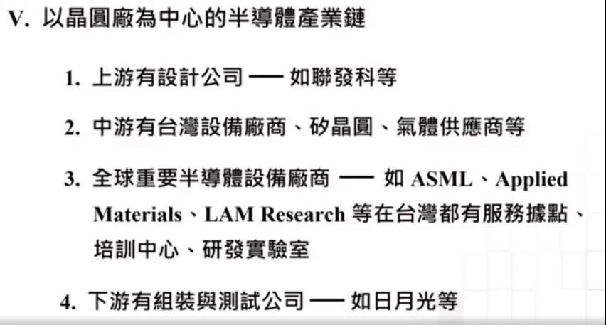
以晶圆厂为中心的半导体产业链

好下一个。那台积电绝对不是只是一个公司,上有设计公司,我只是举个例子,也许是最大的联发科,可是有很多啦。中游有台湾设备厂商,矽晶圆,气体供应商等,raw materials. 还有全球重要的半导体设备商,像ASML, Applied Materials, LAM Research等都在台湾有服务据点、培训中心和研发实验室。所以这些是台积电带过来的,当然我今天是讲台积电,除了它之外台湾还有别的晶圆制造公司。下游有组装与测试公司,这是相当完整的一个产业链。
专业晶圆制造业的创始
专业晶圆制造模式的创始是怎么样的呢?是1985年,事、地、人的巧合,风云际会。事就是工研院的 VLSI 计划,那时已经做了十年,老实说做到了山穷水尽的地步。每年需要很多经费,可是做些小生意就有人说是与民争利。
做了十年了,起初的时候是落后全世界最先进的技术一代而已。75年开始的时候技术从 RCA(美国无线电公司)拿来的,RCA本身也不是第一流的,那个时候拿来的技术就已经是落后的。而做了十年以后,gap差距更大了,两三代了,又是蛮多的经费,养几百人。如果做些小生意,就被accuse为与民争利。
所以李国鼎先生要找出路,我就趁机了。这绝对不是搭便车,foundry model是世界第一个,虽然好处是没有竞争者,坏处是没有客户,那这个我今天不讲了。
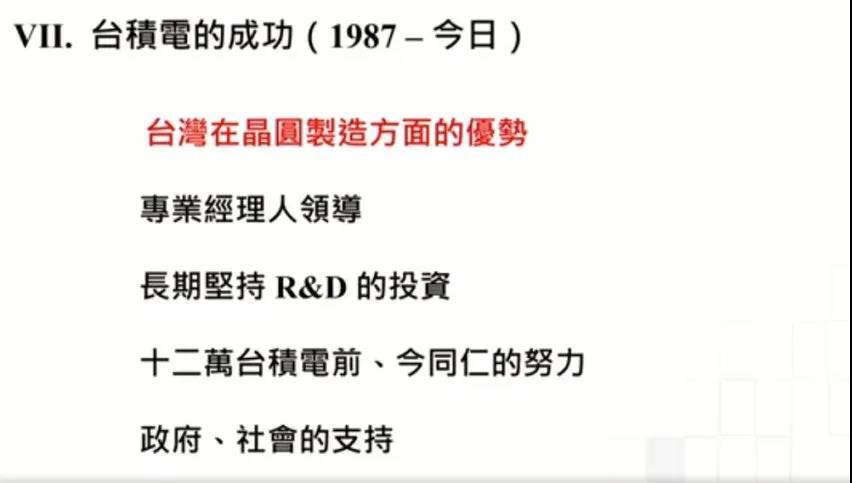
台积电的成功

台积电的成功,为什么,因素是什么?(PowerPoint中)红的是最重要的,就是我刚刚讲到的台湾在晶圆制造方面的优势。
当然专业经理人领导,台积电我想是最大的台湾的公司,是专业经理人领导的,从董事长以下都是专业经理人。当然也有坏处,可是我是觉得,要成立一个世界级的企业,我想专业经理人还是一个比较好的model。
长期坚持 R&D 的投资,这个我们是做到了。
那前前后后,我们有过 12 万员工,这是所有的员工,包括已经离职的。这个其实是离职率很低喔,大概只有 3%、4%。现在就有 5 万员工,三十几年来,12 万员工。
当然政府社会的支持,这也是我今天呼吁的对象,希望他们继续支持台积电,增续在台湾的好处。
台积电今日地位

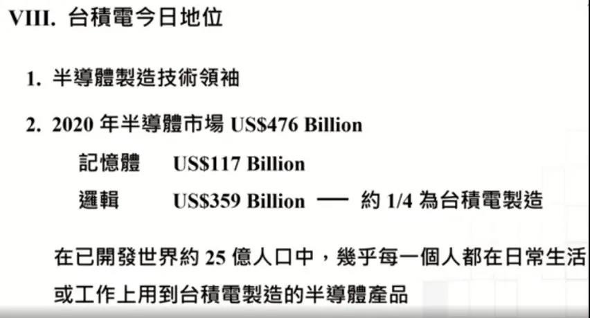
台积电今日地位,半导体制造技术领袖。
半导体市场去年是$476 Billion,当中记忆体是$117 Billion,逻辑是$359 Billion,大约 1/4,其实也不过 1/4 而已,是台积电制造的。
在已开发世界约 25 亿人口中,几乎每个人都在日常生活或工作上用到台积电制造的半导体产品。
例如,其实我是带助听器的,我最近才发现,助听器里面的积体电路(集成电路)也是台积电制造的。
怎么发现的呢?每 3 年他(推销助听器的人员)就过来跟我说出了新型号,要我再买一套。我总是问他new model有什么好处,他讲了一大堆话,后来他讲积体电路换掉了,所以功能会更好的。我居然也是听他的话,也是换了 3、4 个了。
虽然积体电路进步了好几代,但老实说对助听器的功能好像也没什么太大帮助。这有点像美国以前的汽车,每年都有新的model。
美国争取/补贴半导体制造

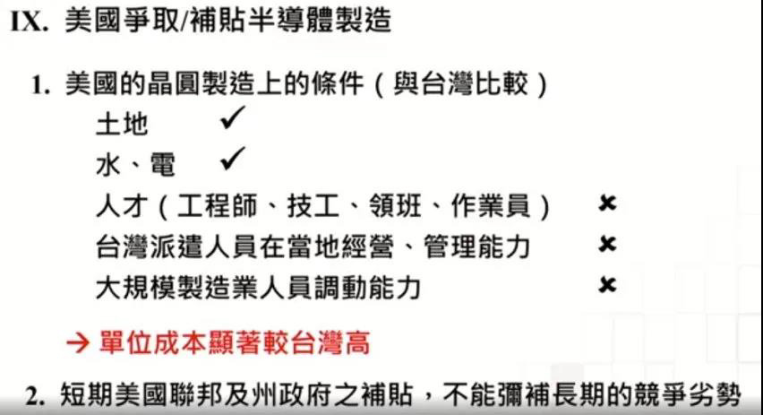
好,看我们竞争的国家,美国最厉害,争取补贴。
美国的晶圆制造条件与台湾比较,土地绝对是占优势,水、电也是占优势。但是我刚刚讲的台湾的优势,美国是弱势。
人才不行,无论工程师、技工、领班、作业员。台湾派遣人员在美国的经营跟管理能力,我刚刚也讲过,未必一流。大规模制造业的人员调动能力也不行。
结果呢,就是单位成本unit cost显著较台湾高。它有补贴啊,这个就是又有胡萝卜,又有棍子。胡萝卜就是联邦政府跟州政府的财政补贴,但是短期的津贴不能够弥补长期的竞争劣势。
它补贴只是几年而已嘛,几年以后你还是要做啊。
大陆的竞争 —— 二十年,数百亿美元补贴之后
下一个,大陆的竞争,20 年,几百亿美元补贴之后,半导体制造落后台积电 5 年以上,逻辑半导体设计落后美国、台湾 1-2 年。
大陆现在还不是对手,尤其在晶圆制造方面,还不是对手。
南韩的竞争 —— 在晶圆制造领域,三星电子是台积电的强劲竞争对手
南韩的竞争,在晶圆制造领域,三星电子是台积电的强劲竞争对手。
为什么?因为南韩在晶圆制造方面优势跟台湾相似,人才也好啦,那三星也是(工厂)都在一个地方,调动人员很方便。
它的经理人也都是韩国人喔,在韩国一流,到国外未必。
台湾下一个“护国神山”
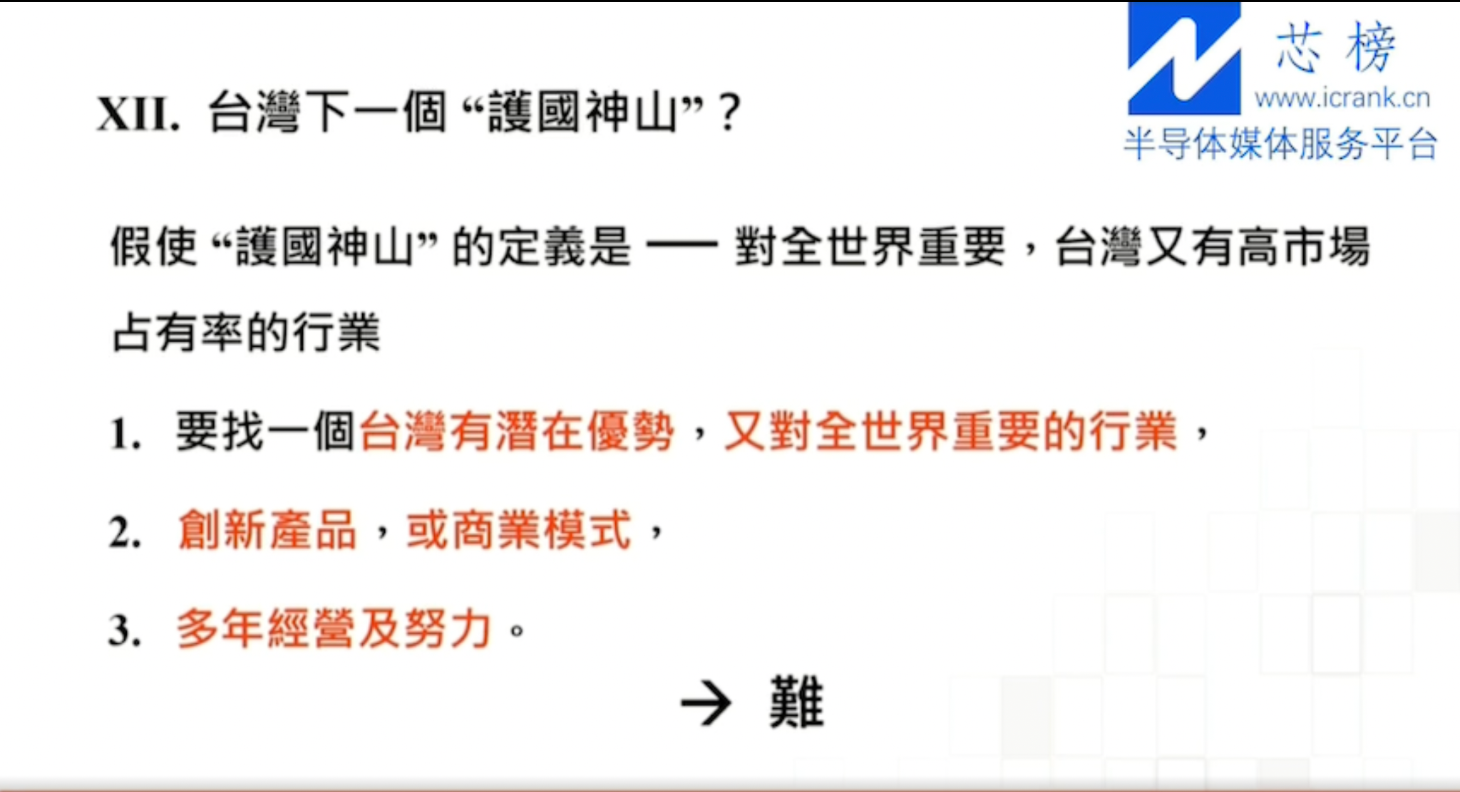
现在有人讲,我们再有一个“护国神山”。假如“护国神山”的定义是对全世界重要,台湾又有高市场占有率的行业,那你要找一个台湾有潜在优势、又对全世界重要的行业。
不然的话,台湾到底也不过只有 2400 万人,地方也小。我找到了一个晶圆制造,我没有再找到,几十年了也没有再找到过。
那下一个“护国神山”要有创新的产品或商业模式,晶圆制造,foundry是一个新的商业模式。
那你也要多年的经营及努力,所以对这个问题,我的答案是:难!
结论

半导体晶圆制造是一个攸关民生、经济、国防的重要产业;它也是第一个台湾在世界竞争力得到相当优势的行业。这优势得来不易,守住亦不易。期望政府、社会、台积电本身,努力把它守住。这是我今天的呼吁,谢谢大家。
如果您喜欢所读的内容,请用email订阅加入“互联”。要想读以前的文章,请查阅《互联档案》。每周一篇新文章送达您的邮箱。请在Twitter、LinkedIn、Clubhouse(@kevinsxu)上给个follow,和我交流互动!